General Description
The RT5760A is a full featured 6V, 1A, Advanced Constant-On-Time (ACOT®) synchronous step-down converter with two integrated MOSFETs. This document explains the function and use of the RT5760A evaluation board (EVB) and provides information for the evaluation board layout, schematic, bill of materials (BOM) and measurement results to suit individual requirements.
Performance Specification Summary
Summary of the RT5760AHGH6F Evaluation Board performance specificiaiton is provided in Table 1. The ambient temperature is 25°C.
Table 1. RT5760AHGH6F Evaluation Board Performance Specification Summary
|
Specification
|
Test Conditions
|
Min
|
Typ
|
Max
|
Unit
|
|
Input Voltage Range
|
|
2.5
|
--
|
6
|
V
|
|
Output Current
|
|
0
|
--
|
1
|
A
|
|
Default Output Voltage
|
|
--
|
1
|
--
|
V
|
|
Operation Frequency
|
|
--
|
2.2
|
--
|
MHz
|
|
Output Ripple Voltage
|
IOUT = 1A
|
--
|
10
|
--
|
mVp-p
|
|
Line Regulation
|
IOUT = 1A, VIN = 2.5V to 6V
|
--
|
±1
|
--
|
%
|
|
Load Regulation
|
VIN = 5V, IOUT = 0.001A to 1A
|
--
|
±1
|
--
|
%
|
|
Load Transient Response
|
IOUT = 0A to 1A
|
--
|
±5
|
--
|
%
|
|
Efficiency
|
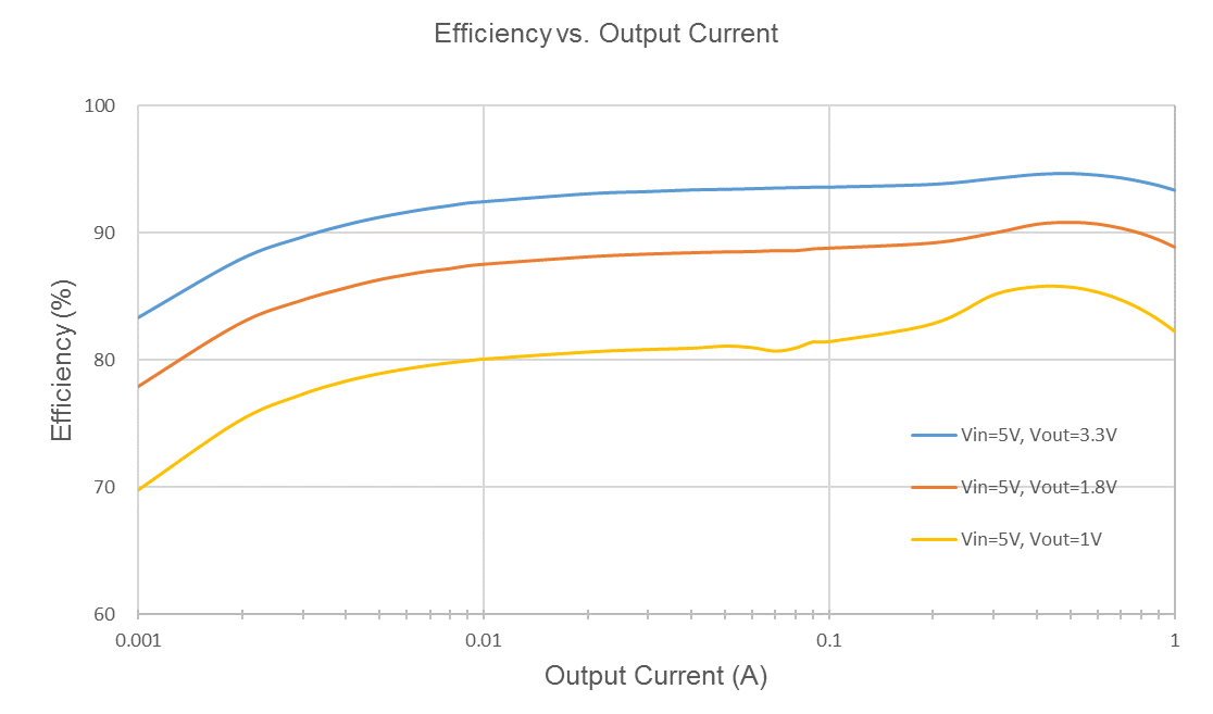
VIN = 5V, VOUT = 1V, IOUT = 0.4A
|
--
|
85.8
|
--
|
%
|
Power-up Procedure
Suggestion Required Equipments
- RT5760AHGH6F Evaluation Board
- DC power supply capable of at least 6V and 1A
- Electronic load capable of 1A
- Function Generator
- Oscilloscope
Quick Start Procedures
The Evaluation Board is fully assembled and tested. Follow the steps below to verify board operation. Do not turn on supplies until all connections are made. When measuring the output voltage ripple, care must be taken to avoid a long ground lead on the oscilloscope probe. Measure the output voltage ripple by touching the probe tip and ground ring directly across the last output capacitor.
Proper measurement equipment setup and follow the procedure below.
1) With power off, connect the input power supply to VIN and GND pins.
2) With power off, connect the electronic load between the VOUT and nearest GND pins.
3) Turn on the power supply at the input. Make sure that the input voltage does not exceeds 60V on the Evaluation Board.
4) Check for the proper output voltage using a voltmeter.
5) Once the proper output voltage is established, adjust the load within the operating ranges and observe the output voltage regulation, ripple voltage, efficiency and other performance.
Detailed Description of Hardware
Headers Description and Placement
Carefully inspect all the components used in the EVB according to the following Bill of Materials table, and then make sure all the components are undamaged and correctly installed. If there is any missing or damaged component, which may occur during transportation, please contact our distributors or e-mail us at evb_service@richtek.com.
Test Points
The EVB is provided with the test points and pin names listed in the table below.
|
Test Point
|
Signal
|
Comment (expected waveforms or voltage levels on test points)
|
|
VIN
|
Input Voltage
|
Positive input voltage from the power supply to the EVB.
|
|
VOUT
|
Output Voltage
|
Positive output voltage from the EVB to the loads.
|
|
JP1
|
Output Voltage Test Point
|
Output voltage measurement point.
|
|
GND
|
Ground
|
Reference voltage for input voltage, output voltage and other test points.
|
|
LX
|
Switch Node Test Point
|
Frequency measurement point. 2.2MHz (Typ.) in CCM mode.
|
|
PG
|
Power Good Test Point
|
Power good indicator. Pull low for fault condition.
|
|
EN
|
Enable Test Point
|
Enable control input. Connect this pin to logic high to enable the device.
|
|
JP2
|
EN Pin Jumper
|
Place the jumper across on EN and H to enable the device. Place the jumper across on EN and L to disable the device.
|
Power-up & Measurement Procedure
1. Connect a input power supply to the VIN and GND terminals and an electrical load to the VOUT and GND terminals.
2. Set the jumper at JP2 to tie “EN” test pin to “H” pin for enabling the chip.
3. Apply a 5V nominal input power supply (2.5V < VIN < 6V) to the VIN and GND terminals respectively.
4. Set the electrical load up to 1A to Verify the output voltage (approximately 1V) at JP1. Check LX frequency is around 2.2MHz in CCM mode.
Output Voltage Setting
Set the output voltage with the resistive divider (R1, R2) between VOUT and GND with the midpoint connected to FB. The output is set by the following formula :

The placement of the resistive divider should be within 5mm of the FB pin. The resistance of R2 is suggested to 10kΩ for noise pick-up at the FB pin. The resistance of R1 can then be obtained as below :

For better output voltage accuracy, divider resistors (R1 and R2) should have tolerance of ±1% tolerance or better.
Bill of Materials
|
Reference
|
Qty
|
Part Number
|
Description
|
Package
|
Manufacturer
|
|
U1
|
1
|
RT5760AHGH6F
|
Step-Down
DC-DC Converter
|
SOT-563
|
WALSIN
|
|
C1, C4, C5
|
3
|
|
NC
|
C-0603
|
|
|
C2, C6
|
2
|
0603X106M6R3CT
|
10µF/6.3V/X5R/0603
|
C-0603
|
WALSIN
|
|
C3
|
1
|
C1005X7R1C104K050BC
|
100nF/16V/X7R/0402
|
C-0402
|
TDK
|
|
C7
|
1
|
C1608X7R1H104K080AA
|
100nF/50V/X7R/0603
|
C-0603
|
TDK
|
|
L1
|
1
|
DFE252010F-1R0M
|
1µH
|
L-2520
|
Murata
|
|
R1
|
1
|
WR06X6651FTL
|
6.65K/0603
|
R-0603
|
WALSIN
|
|
R2
|
1
|
WR06X1002FTL
|
10K/0603
|
R-0603
|
WALSIN
|
|
R3, R4
|
2
|
WR06X1003FTL
|
100K/0603
|
R-0603
|
WALSIN
|
|
R5
|
1
|
|
NC
|
R-0603
|
|
|
R6
|
1
|
WR06X000 PTL
|
0/0603
|
R-0603
|
WALSIN
|
Typical Applications
EVB Schematic Diagram
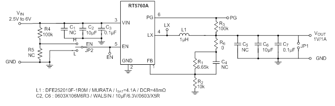
Note:
1. Do not hot-plug a live 5V supply to the board. If hot-plugging is required, add ~ 100µF electrolytic capacitor at the input.
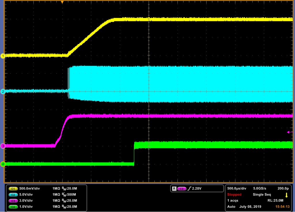
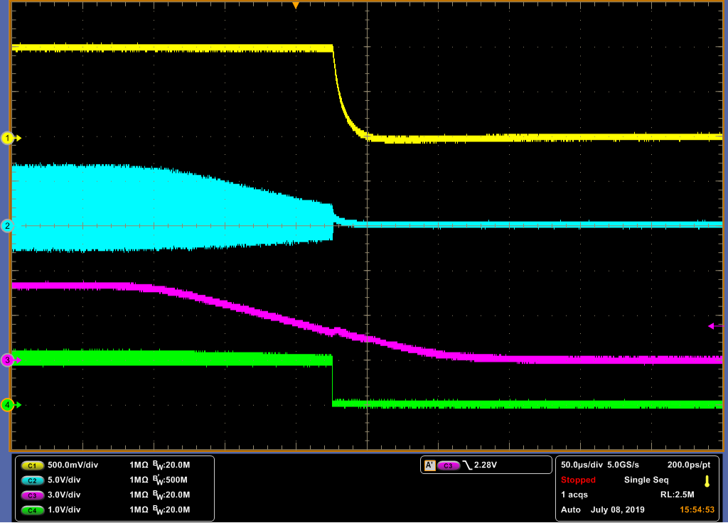
Measurement Results
|
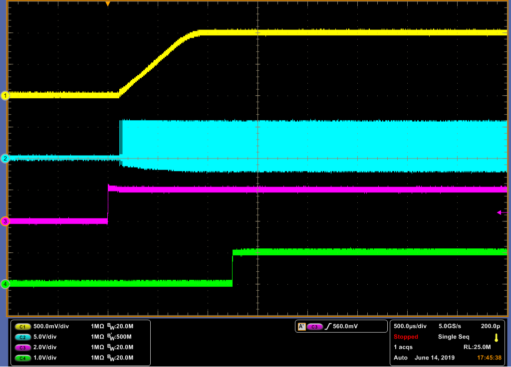
Power-On from VIN
Yellow: VOUT; Cyan: LX; Pink: VIN; Green: PG
|
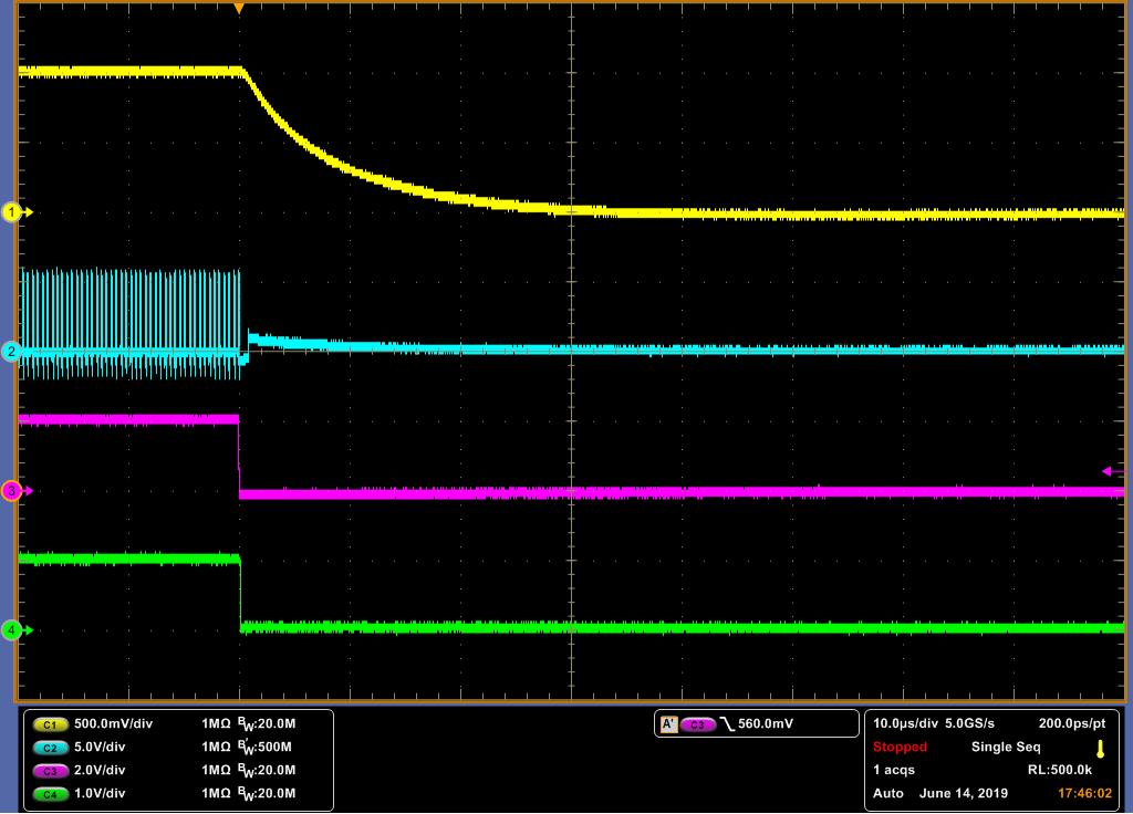
Power-Off from VIN
Yellow: VOUT; Cyan: LX; Pink: VIN Green: PG
|
|
|
|
|
VIN = 5V, VOUT = 1V, IOUT = 1A
|
VIN = 5V, VOUT = 1V, IOUT = 1A
|
|
Power-On from EN
Yellow: VOUT; Cyan: LX; Pink: EN; Green: PG
|
Power-Off from EN
Yellow: VOUT; Cyan: LX; Pink: EN; Green: PG
|
|
|
|
|
VIN = 5V, VOUT = 1V, IOUT = 1A
|
VIN = 5V, VOUT = 1V, IOUT = 1A
|
|
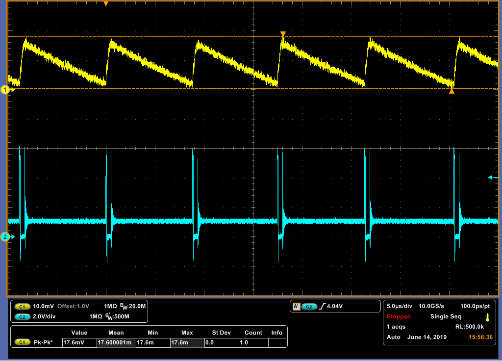
Output Ripple Measurement
Yellow: VOUT; Cyan: LX
|
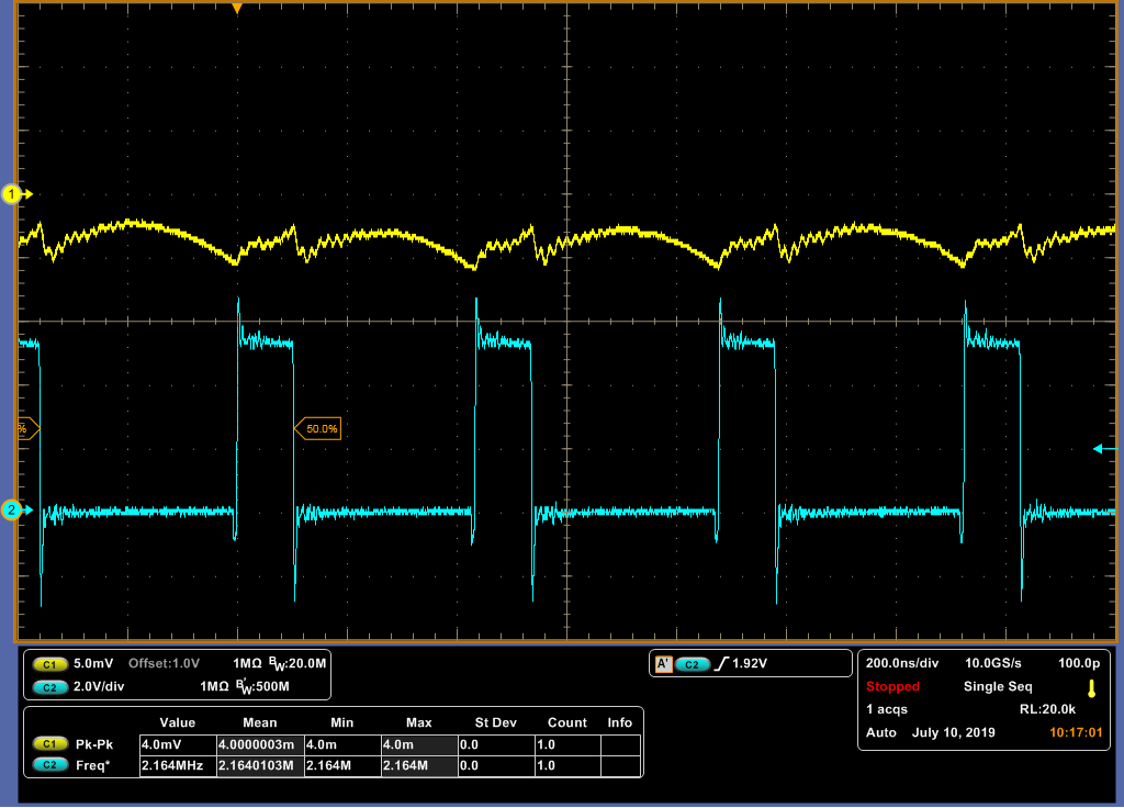
Output Ripple Measurement
Yellow: VOUT; Cyan: LX
|
|
|
|
|
VIN = 5V, VOUT = 1V, IOUT = 0.01A
Output ripple: 17.6mVpp (PSM)
|
VIN = 5V, VOUT = 1V, IOUT = 1A
Output ripple: 4mVpp, Frequency: 2.164MHz (CCM)
|
|
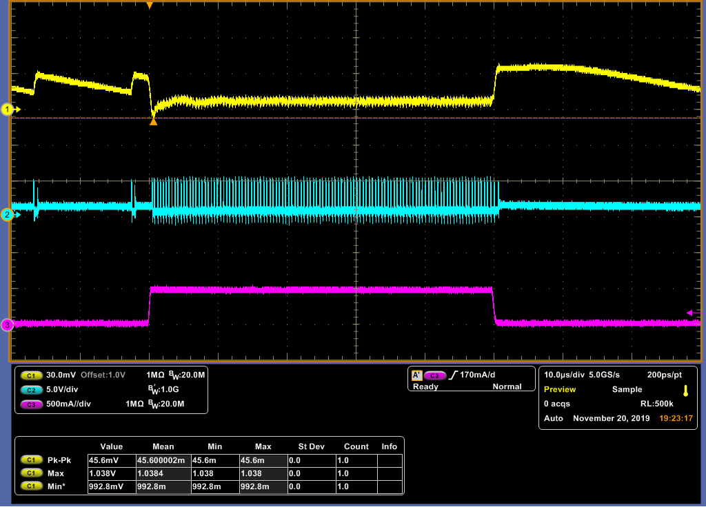
Fast Dynamic Load
Yellow: VOUT; Cyan: LX; Pink: IOUT
|
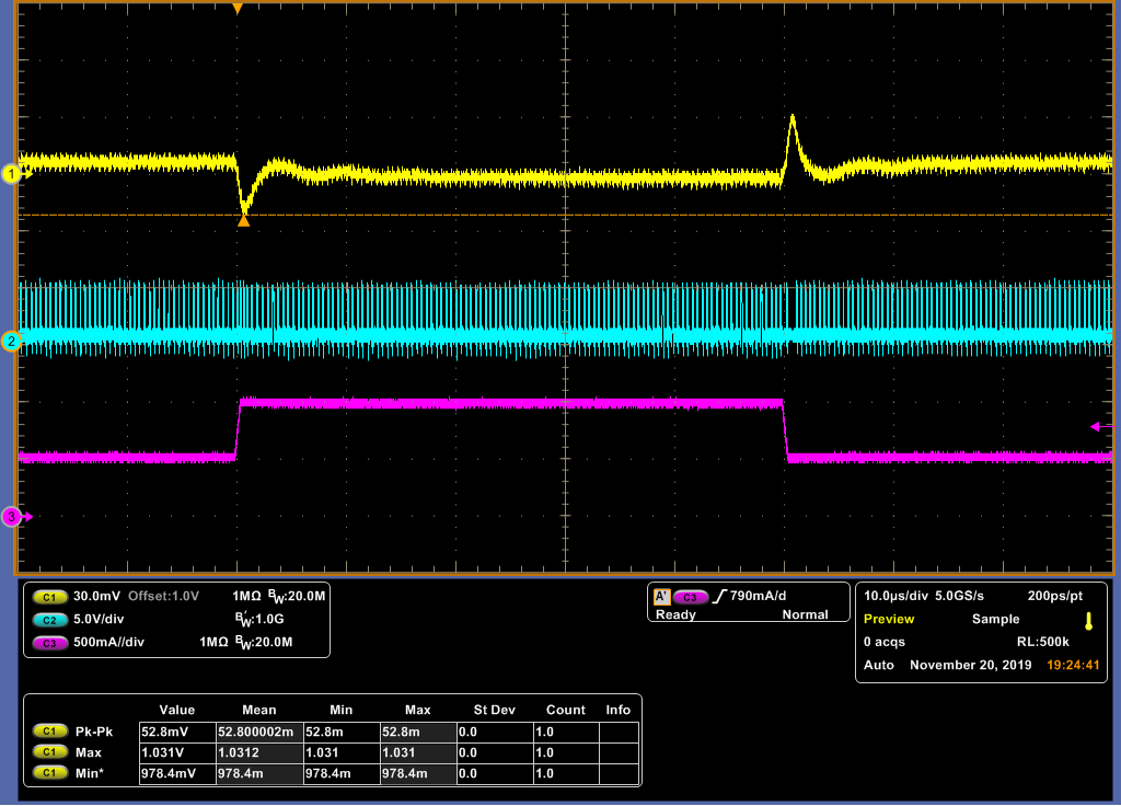
Fast Dynamic Load
Yellow: VOUT; Cyan: LX; Pink: IOUT
|
|
|
|
|
VIN = 5V, VOUT = 1V, IOUT = 0.01A to 0.5A (SR = 1A/µs)
Output ripple: 45.6mVpp
|
VIN = 5V, VOUT = 1V, IOUT = 0.5A to 1A (SR = 1A/µs)
Output ripple: 52.8mVpp
|
|
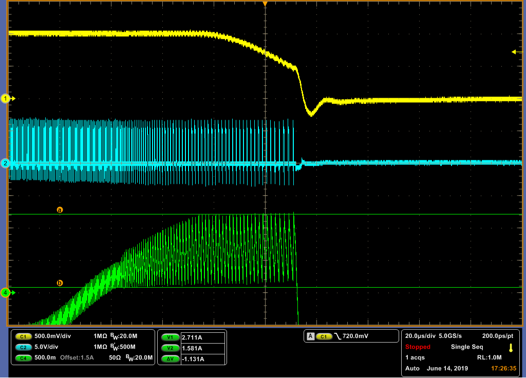
OCP Function
Yellow: VOUT; Cyan: LX; Green: Inductor current
|
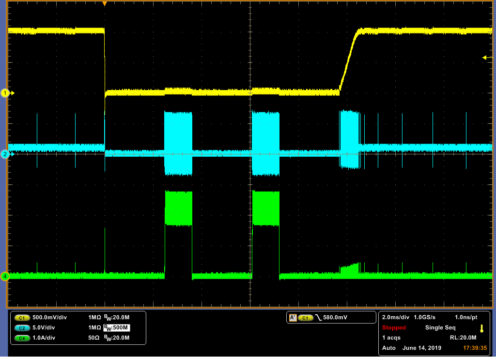
UVP Function
Yellow: VOUT; Cyan: LX; Green: Inductor current
|
|
|
|
|
VIN = 5V, VOUT = 1V, IOUT = 0A to OCP (Gradually increase load)
Low-side current limit is 1.581A
High-side current limit is 2.711A
|
VIN = 5V, VOUT = 1V, IOUT = 0A (Output short and recovery)
|
|
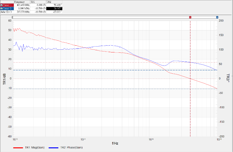
Bode Plot
|
|
|
|
|
|
VIN = 5V, VOUT = 1V, IOUT = 1A
Bandwidth = 402kHz
Phase Margin = 56.4
|
|
Efficiency Measurements
Evaluation Board Layout
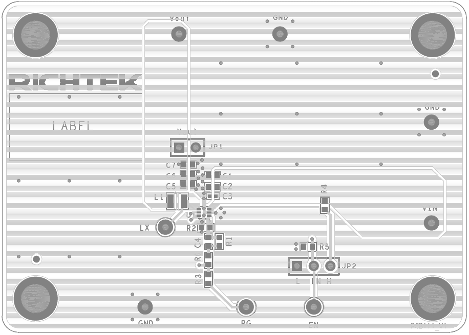
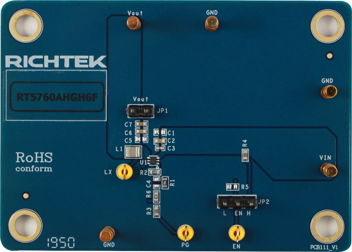
Figure 1. Top View (1st layer)
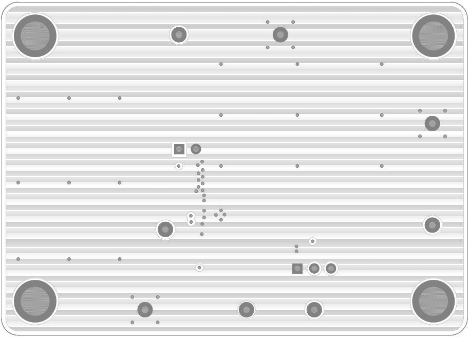
Figure 2. PCB Layout—Inner Side (2nd Layer)
Figure 3. PCB Layout—Inner Side (3rd Layer)
Figure 4. Bottom View (4th Layer)